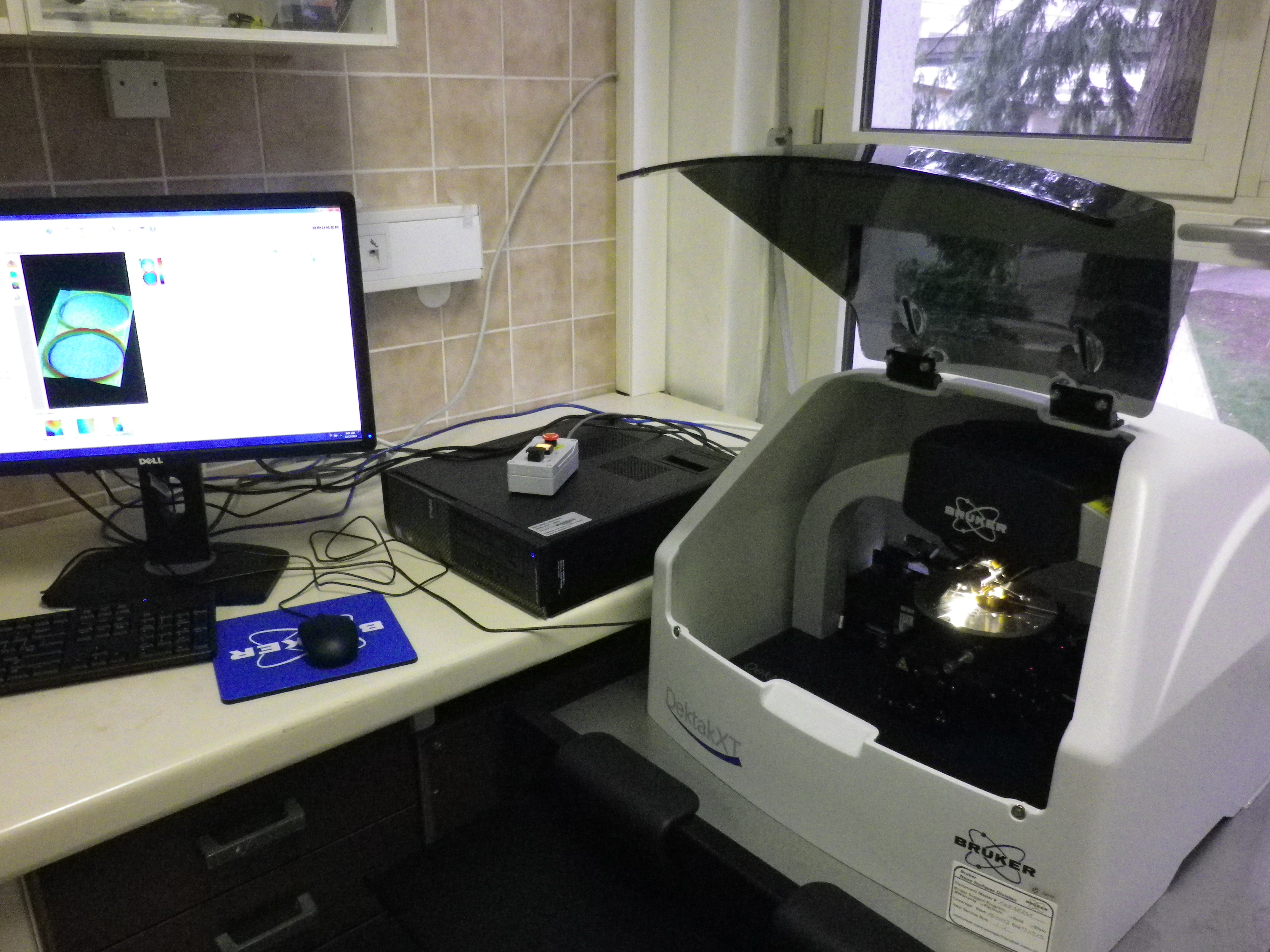
type: Bruker Dektak XT
producer: Bruker Corp., Billerica, USA
resolution: 3 nm in x-direction, 1 μm in y-direction, 0.1 nm in z-direction
It is dedicated to smaller samples with a flat geometry where a better resolution is required.
The device measures the surface profile. From a line profile z(x) we can calculate the roughness parameters (Ra, Rt, Rz, etc), coating thickness (if part of the sample was previously covered by a mask) and internal stress. In 3D mode the result is the surface topography, which can be presented as an image, or it can be used to calculate various parameters: roughness, wear volume, defect density, surface texture, etc.
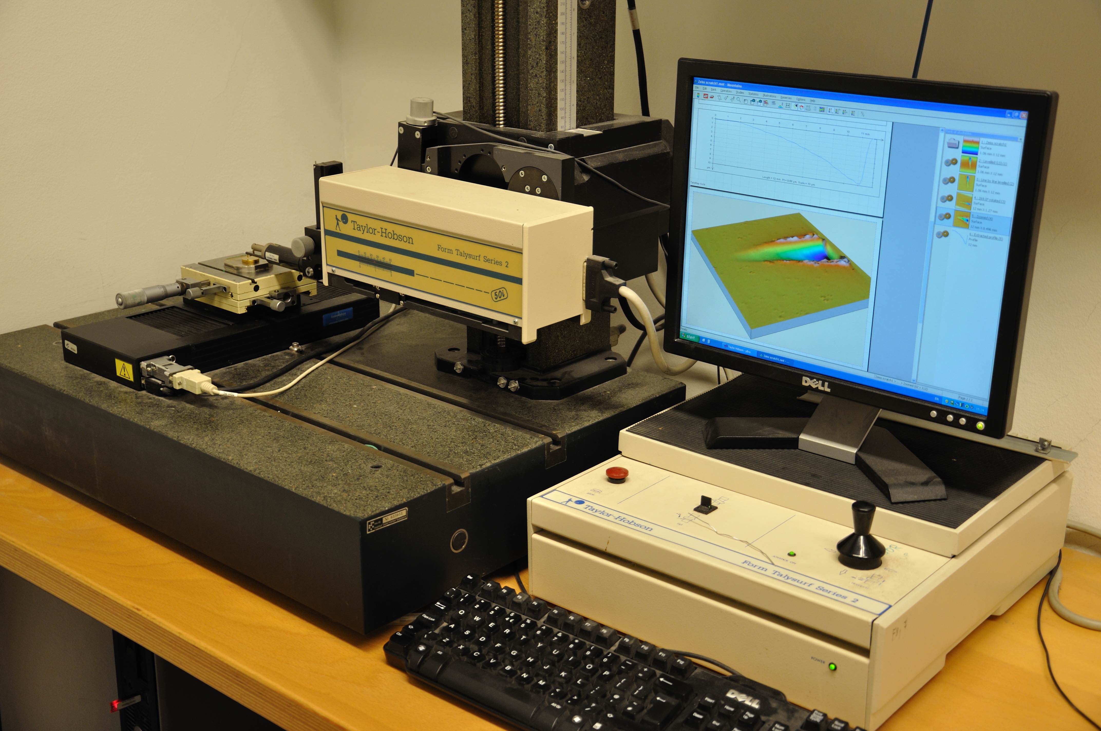
type: Form Talysurf Series 2
producer: Taylor-Hobson Ltd., Leicester, UK
resolution: 0.25 μm in x-direction, 1 μm in y-direction, 3 nm in z-direction
It is dedicated to samples with a complicated geometry and of greater size (tools also), however, the resolution is somewhat coarse.
![]()
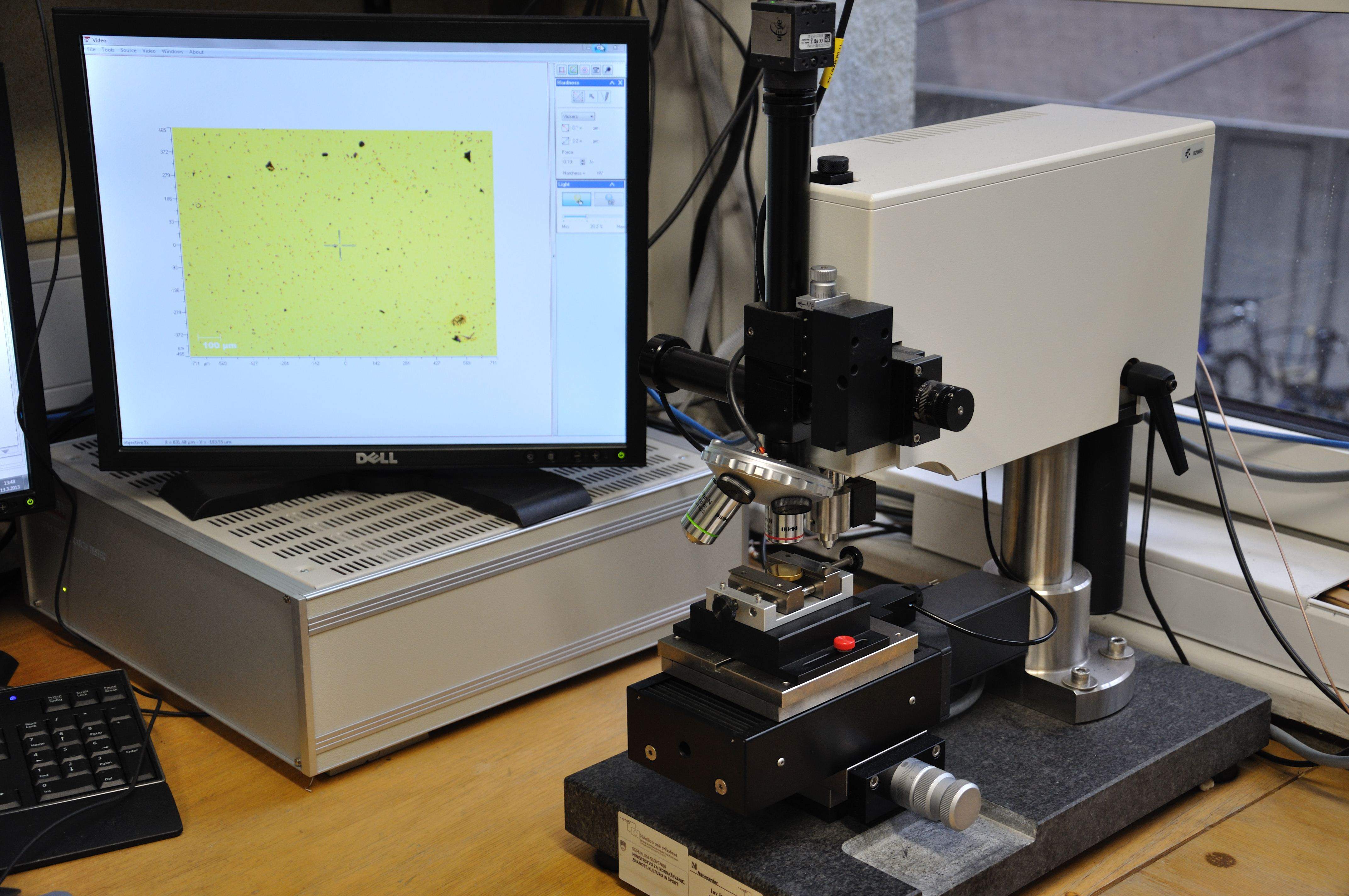
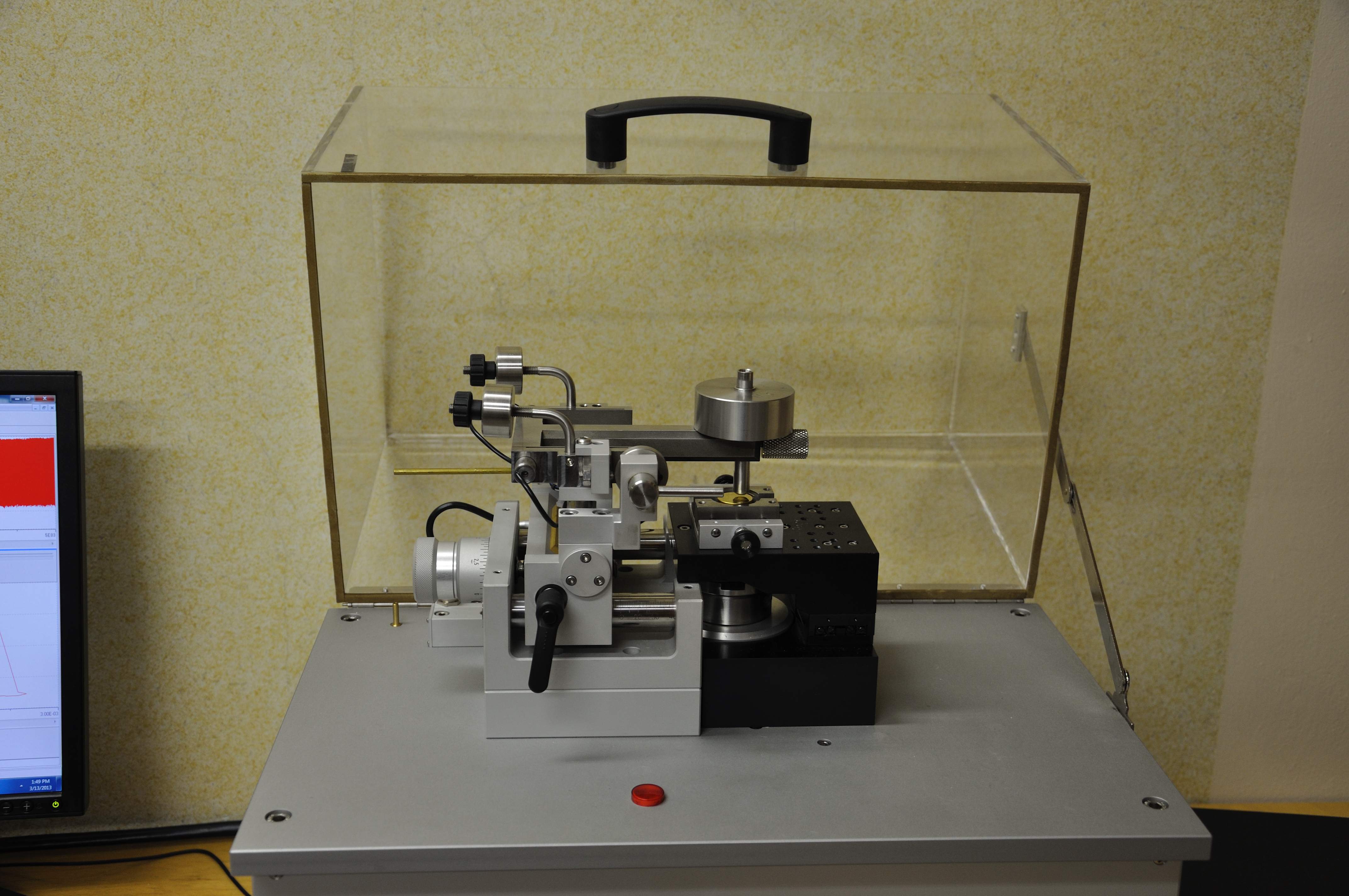
The device is used to evaluate the adhesion of the coating on the substrate based on the scratch test principle. A diamond tip slides on the sample surface, while the load is linearly increased. The device records the scratching force, the tip penetration depth and the acoustic emission, while the scratch track is afterwards evaluated by optical microscopy. The criterion for adhesion are the critical loads, where specific pre-defined coating failures appear.
type: Revetest Scratch tester
producer: CSM Instruments, Neuchatel, Switzerland
maximum load: 200 N, measurement length: 1 cm
The apparatus is owned by the center of excellence Nanocenter.
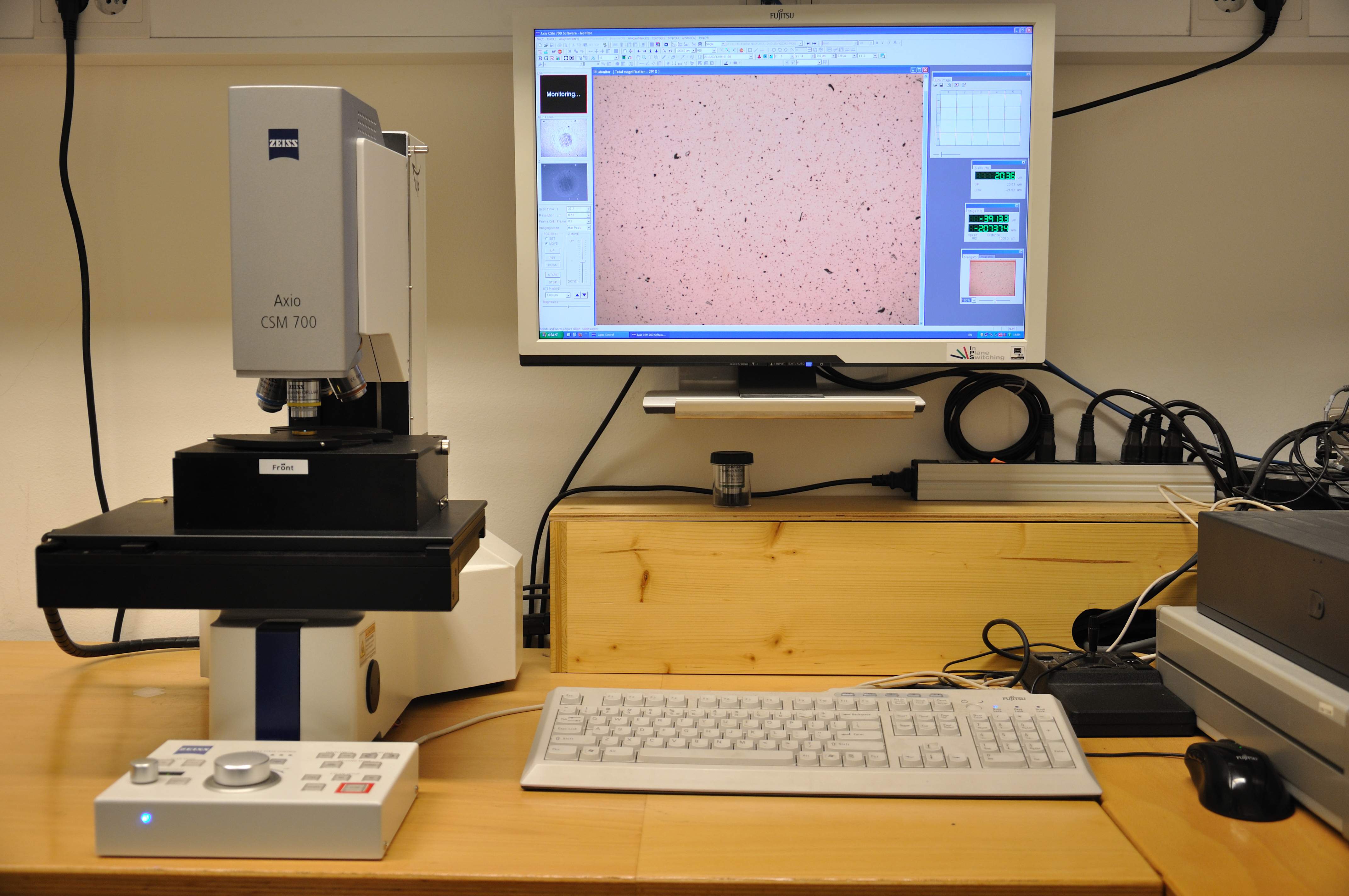
The microscope acquires the image of the sample surface which can be presented in two ways:
(i) all-in-focus image and
(ii) surface topography. From the topographic image one can calculate the roughness, coating thickness, wear volume, etc.
type: Axio CSM 700
producer: Zeiss, Jena, Germany
magnification: 30x up to 1500x
image size: 100 μm up to 5 mm
This concerns the measurement of the "pin on disk" type, where a standard tip slides on the sample surface. The sliding may be circular or linear, can be performed in air or in liquid, in a range between room temperature and 170 °C. The device records the friction coefficient, while the tip wear track cross-section can be used to calculate the wear volume.
type: Tribometer
producer: CSM Instruments, Neuchatel, Switzerland
maximum load: 10 N
The apparatus is owned by the center of excellence Nanocenter.
![]()
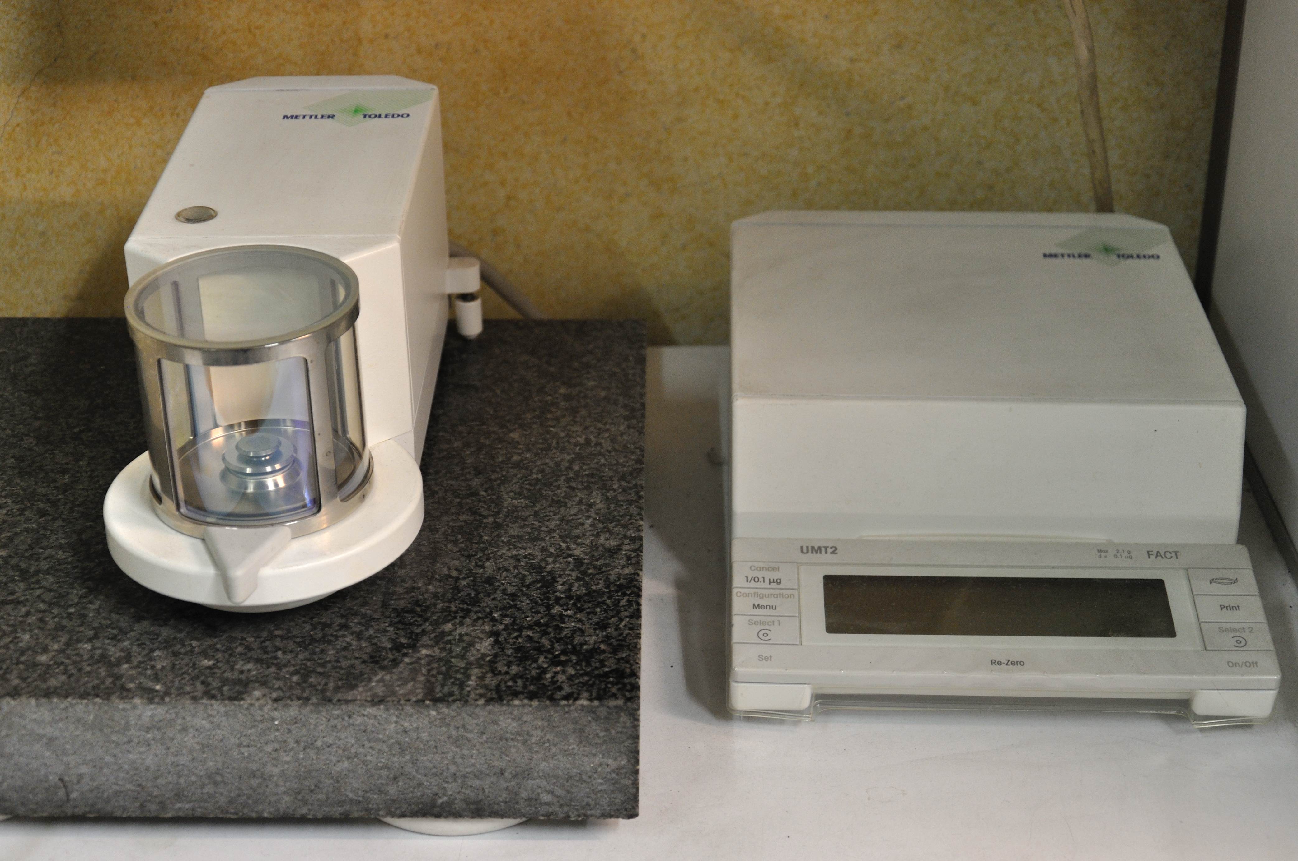
Using a microbalance we measure the surface mass of a thin film, and indirectly the thin film density. By measuring the sample weight gain during annealing in an oxygen atmosphere we can observe the oxidation kinetics.
type: UMT 2
producer: Mettler Toledo, Greifensee, Switzerland
resolution: 0.1 μg, maximum load: 2 g
![]()
![]()
Vickers
nanohardness tester
Applied for advanced analysis of
thin film mechanical properties.
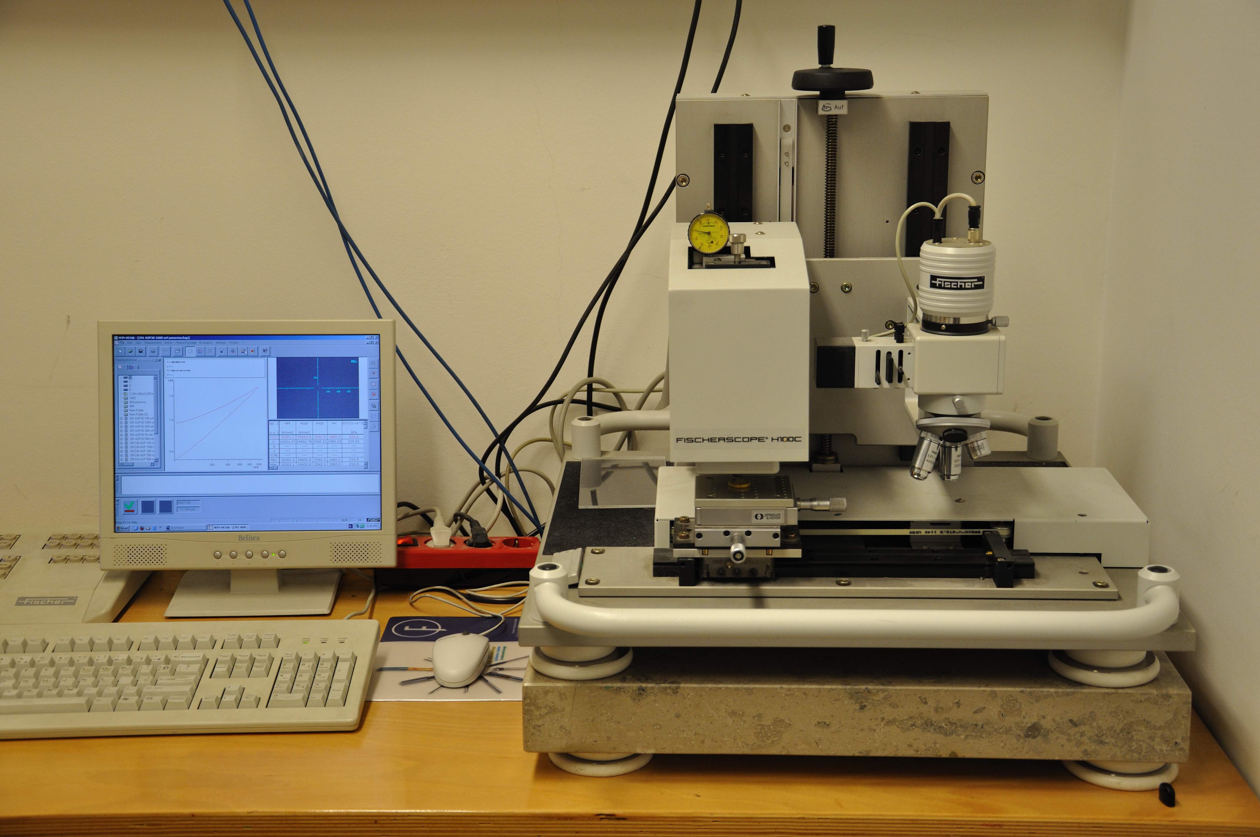
type: Fischerscope H100C
producer: Helmut Fischer, Sindelfingen-Maichingen, Germany
load range: 0.4 mN–1 N (40 mg–100 g)
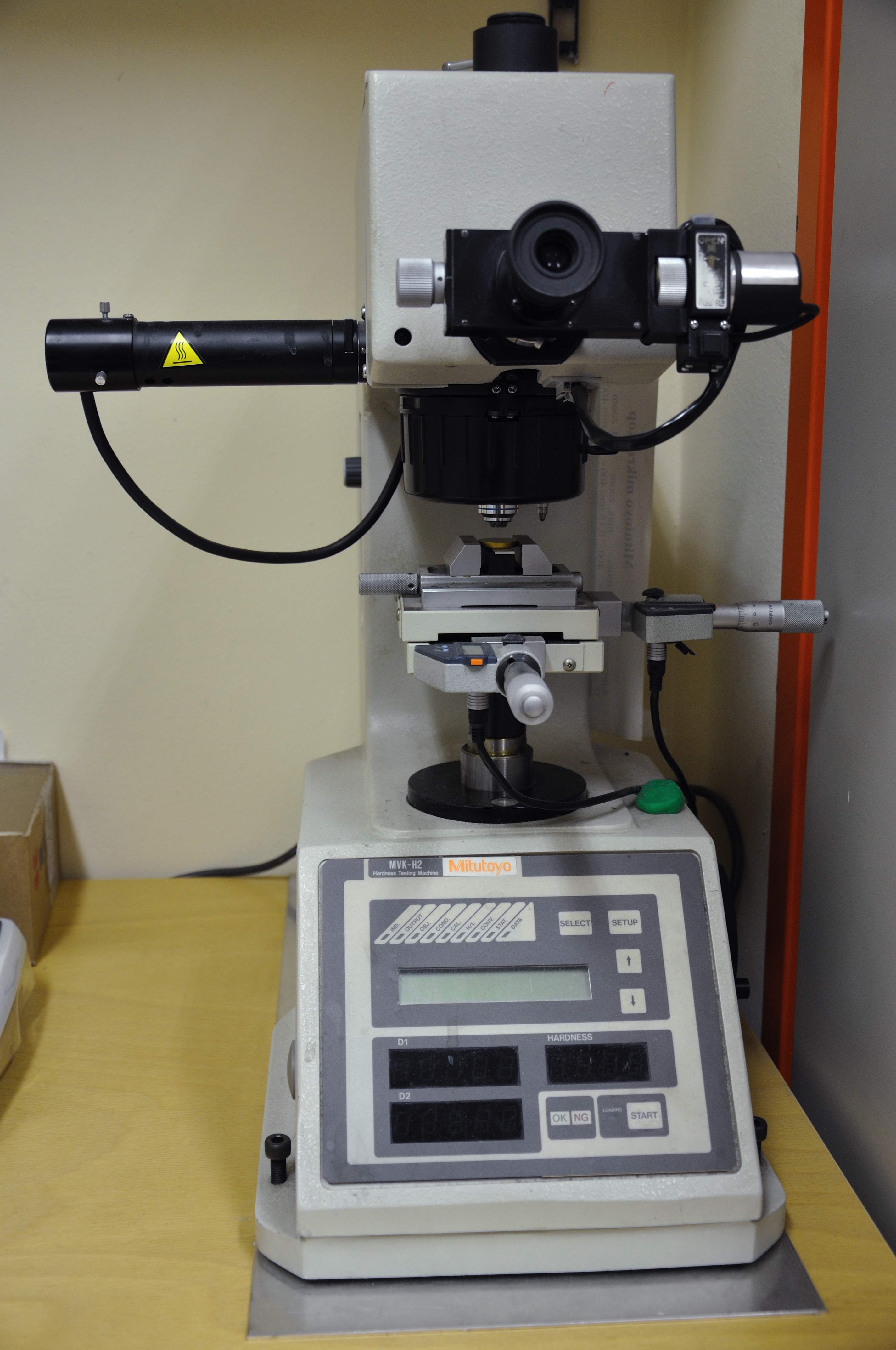
type: MVK-H2 Hardness tester
producer: Mitutoyo, Kawasaki, Japonska
load range: 10 mN–20 N (1 g–2 kg)
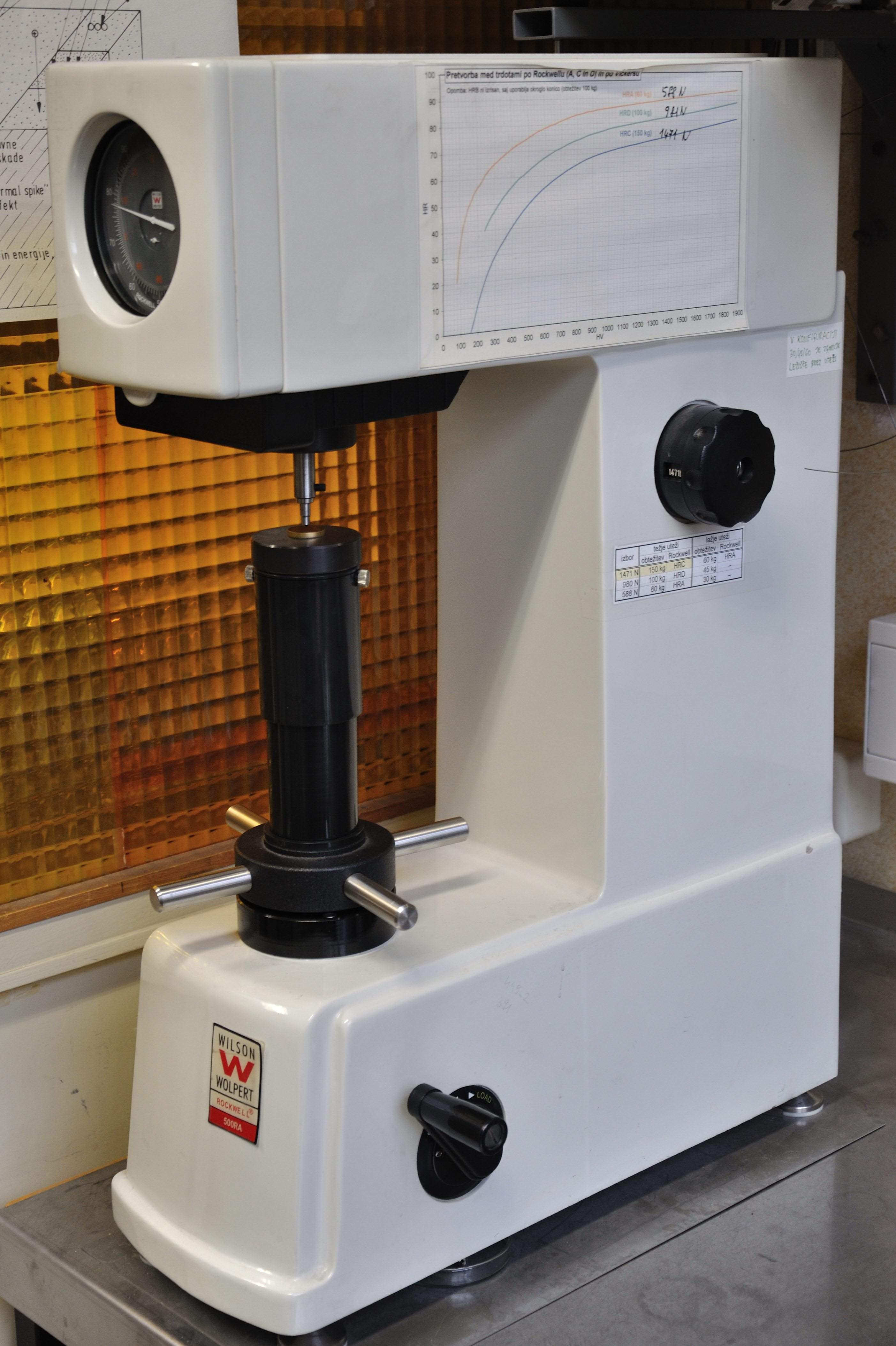
type: Rockwell 500RA
producer: Wolpert Wilson Instruments, Boston, USA
load range: 300–1500 N (30–150 kg)
![]()